
When the Curve Flattens: Semiconductor Technologies Approaching Their 2026 Inflection
By 2026, several semiconductor technologies will reach a point where incremental gains no longer justify exponential complexity. This is not a collapse, but a maturing of curves that have been aggressively bent over the last decade. What follows is a period of optimization, selective investment, and architectural rethinking rather than raw scaling. Understanding which technologies are peaking—and why—matters because it reshapes capital allocation, talent focus, and long-term competitiveness.
Advanced Logic Nodes and the End of Easy Scaling
 Leading-edge logic will continue to advance past the current nodes, but the nature of progress changes sharply around the mid-2020s. Transistor density improvements increasingly come from layout tricks, device stacking, and design-technology co-optimization rather than fundamental lithographic breakthroughs. Gate-all-around structures reduce leakage and improve control, yet variability, parasitic resistance, and thermal coupling become dominant limiters. Power delivery networks struggle to keep pace with switching density, even as backside power techniques are introduced.
By 2026, the industry reaches a point where performance-per-watt gains are real but narrow, and cost-per-transistor improvements flatten. Design complexity, mask counts, and verification effort explode, making only the highest-volume or most strategic designs economically viable at the leading edge. The node race continues, but its strategic impact diminishes.
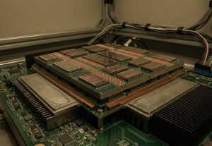
HBM Scaling and the Memory Wall Revisited
 High-bandwidth memory has been one of the most important enablers of AI acceleration, but its current trajectory also faces constraints. Stacking depth increases, signaling speeds rise, and interposer complexity grows, yet yield sensitivity and thermal density tighten the margins. Power delivery into stacked dies becomes non-trivial, and marginal bandwidth gains demand disproportionate packaging sophistication.
Around 2026, HBM evolution shifts from aggressive bandwidth chasing to efficiency, reliability, and system-level optimization. Architects begin trading raw throughput for smarter data movement, compression, and locality-aware compute. The memory wall does not disappear—it becomes more expensive to push back.
Chiplets: From Differentiator to Default
 Disaggregated design has rapidly moved from experimental to mainstream. Chiplets unlock yield improvements, faster time-to-market, and heterogeneous integration across process nodes. However, by the mid-decade, chiplet architectures stop being a competitive differentiator and start becoming table stakes.
The limiting factors emerge elsewhere: die-to-die interconnect standards, coherency overhead, test complexity, and system validation. As packaging density increases, signal integrity and thermal coupling constrain layout freedom. The innovation focus shifts from “can we disaggregate?” to “how efficiently can we orchestrate disaggregated systems at scale?” By 2026, chiplets peak as a novelty and settle into infrastructure.
EUV Maturity and Lithography Saturation
 Extreme ultraviolet lithography remains indispensable, but its role subtly changes. Tool productivity improves, defectivity decreases, and patterning flows stabilize. However, each incremental resolution gain demands disproportionate investment in optics, source power, and process control. Multipatterning does not vanish; it reappears in different guises.
By 2026, lithography is no longer the pacing item for innovation—it becomes a cost anchor. The industry accepts that lithographic heroics deliver diminishing strategic returns compared to architectural and packaging advances.
Monolithic SoCs and the Limits of Integration
 The era of ever-larger monolithic system-on-chip designs approaches its practical limits. Reticle size constraints, yield loss, and escalating design cycles make extreme integration unattractive for anything but the most controlled ecosystems. Verification complexity grows faster than transistor counts, and late-stage changes become prohibitively risky.
As a result, integration shifts upward in the stack—into packages, platforms, and software-defined composition. By 2026, the monolithic SoC peaks as a design philosophy, replaced by modularity as the dominant paradigm.
What Peaks Do—and Do Not—Mean
 A technology peaking does not imply irrelevance. It signals a transition from expansion to extraction—maximizing value from what already exists. Capital shifts from brute-force scaling to yield learning, reliability engineering, and workload-specific optimization. Talent moves from pure device physics into cross-layer roles spanning architecture, packaging, and software.
The next phase of semiconductor leadership will not come from pushing any single curve harder, but from synchronizing many curves well enough that systems behave coherently under real workloads.
After the Peak
By 2026, semiconductors enter a phase where progress feels quieter but becomes more consequential. Fewer breakthroughs make headlines, yet more decisions lock in long-term advantage. The frontier moves from “smaller and faster” to “better aligned and more efficient.” In that transition, the winners will be those who understand not just how technologies peak, but how to build enduring value on the plateau that follows.

