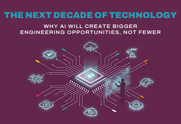
Pioneering India's Semiconductor Future: A Landmark MoU for the First Private SiC Fab in Andhra Pradesh

Pioneering India’s Semiconductor Future: A Landmark MoU for the First Private SiC Fab in Andhra Pradesh

Pioneering India’s Semiconductor Future: A Landmark MoU for the First Private SiC Fab in Andhra Pradesh We at BITSILICA are excited to share a monumental leap forward for India’s semiconductor industry. Indichip Semiconductors Limited, alongside their joint venture partner Yitoa Micro Technology Limited (YMTL) from Japan, has inked a Memorandum of Understanding (MoU) with the […]
Read More

Transformative Trends in the Semiconductor Industry: Redefining Technology for 2025

Transformative Trends in the Semiconductor Industry: Redefining Technology for 2025 As 2025 approaches, the semiconductor industry stands on the brink of a transformative phase, driven by unprecedented advancements in artificial intelligence (AI), cutting-edge chip packaging techniques, and next-generation power components. These innovations are not just reshaping the industry but are also enabling smarter, faster, and […]
Read More
Functional-ECOs-The-Key-to-Efficient-and-Adaptive-Chip-Design

Functional ECOs: The Key to Efficient and Adaptive Chip Design

Functional ECOs: The Key to Efficient and Adaptive Chip Design In chip design, Engineering Change Orders (ECOs) exemplify innovation and adaptability. Among these, Functional ECOs enable targeted modifications to a chip’s logical structure without restarting the entire process. They address critical bugs, accommodate feature changes, and optimize design behavior while maintaining logical integrity and meeting […]
Read More
BITSILICA Receives Partner Par Excellence Award from Qualcomm

Partner Par Excellence Award from Qualcomm

BITSILICA Receives “Partner Par Excellence” Award from Qualcomm We are thrilled to share a momentous achievement with our valued network! BITSILICA has been honored with the prestigious “Partner Par Excellence” award from Qualcomm. This recognition underscores our unwavering commitment to delivering world-class quality in both our services and solutions. At BITSILICA, we believe that true […]
Read More
Unlocking Memory Efficiency in Data Centers with CXL

Unlocking Memory Efficiency in Data Centers with CXL

Unlocking Memory Efficiency in Data Centers with CXL As data centers evolve to meet the demands of rapidly advancing technologies like artificial intelligence (AI), machine learning (ML), and real-time analytics, the need for efficient and scalable memory management has never been more critical. Compute Express Link (CXL) is emerging as a transformative solution, offering innovative […]
Read More
The Shift to 3D-IC: A New Era For Backend Design Engineers

The Shift to 3D-IC: A New Era For Backend Design Engineers

The Shift to 3D-IC: A New Era For Backend Design Engineers   The semiconductor industry’s shift from traditional 2D scaling to three-dimensional integrated circuits (3D-ICs) is transforming chip design. By stacking silicon layers vertically, 3D-ICs deliver significantly higher device density, performance, and energy efficiency—all essential for advancing AI, high-speed computing, and mobile technologies. However, while […]
Read More

Challenges Facing Autonomous Vehicles: Current Trends and Innovations

Challenges Facing Autonomous Vehicles: Current Trends and Innovations Autonomous vehicles (AVs) are at the forefront of technological innovation, promising to revolutionize transportation by improving safety, efficiency, and convenience. However, despite significant advancements, several challenges need to be addressed to ensure the widespread adoption and safe operation of AVs. This blog explores the key challenges facing […]
Read More
Challenges Facing Autonomous Vehicles: Current Trends and Innovations

Understanding Tapeout: A Crucial Milestone in the Semiconductor Industry

Understanding Tapeout: A Crucial Milestone in the Semiconductor Industry Tapeout is a critical milestone in the semiconductor design and manufacturing process. It represents the final step before a chip design is sent to a fabrication plant (fab) for manufacturing. For young professionals and enthusiasts in the semiconductor industry, understanding tapeout is essential. Tapeout Tapeout refers […]
Read More
The Role of Place and Route in VLSI Physical Design

The Role of Place and Route in VLSI Physical Design

The Role of Place and Route in VLSI Physical Design Physical design is converting a gate-level netlist into a GDSII format, where the logical connectivity of cells is transformed into physical connectivity.  The main goals of physical design are  1. Optimizing Power,  2. Performance, and  3. Area.  Place and route play a crucial role in […]
Read More
Optimising Power Efficiency in SoC Designs A Guide to Low Power Verification

Optimising Power Efficiency in SoC Designs A Guide to Low Power Verification

Optimising Power Efficiency in SoC Designs: A Guide to Low Power Verification Power consumption is among the most essential design metrics in current Silicon-On-Chip (SoC) designs. Using low power verification, the users can significantly reduce the power consumption of design by defining the power-aware strategies using Unified Power Format with design at different levels: simulation […]
Read More