

How Open Die-to-Die Interconnects Are Reshaping the Semiconductor Industry
Introduction
The semiconductor industry is undergoing a major architectural transition. For decades, increasing computing performance largely depended on putting more transistors onto a single monolithic chip. However, modern applications such as Artificial Intelligence (AI), High-Performance Computing (HPC), data centers, networking, and advanced communications are demanding enormous increases in compute performance, memory bandwidth, and energy efficiency.
At the same time, manufacturing extremely large monolithic chips has become increasingly expensive and technically challenging.
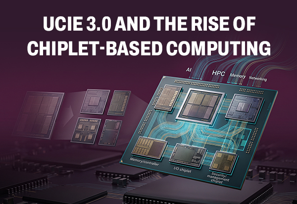
This cost and yield pressure has accelerated the adoption of chiplet-based architectures, where a complex system is divided into multiple smaller dies called chiplets and integrated together inside a single package.
A key technology enabling this transition is UCIe — Universal Chiplet Interconnect Express. UCIe defines an open, standardized die-to-die interconnect that allows chiplets to communicate efficiently within a package.
The release of UCIe 3.0 in August 2025 represents an important step in this evolution. UCIe 3.0 supports 48 GT/s and 64 GT/s data rates, doubling the maximum data rate compared with UCIe 2.0’s 32 GT/s, while adding improvements in power efficiency, manageability, sideband communication, and system flexibility.
1. What Is a Chiplet?

A chiplet is a small semiconductor die designed to perform a specific function within a larger system.
Instead of building one large SoC containing everything, designers can divide the system into multiple chiplets.
For example, an AI processor could contain:
- CPU chiplets
- GPU/AI accelerator chiplets
- I/O chiplets
- Memory controller chiplets
- Security chiplets
- Networking chiplets
- Cache chiplets
These chiplets are integrated into the same advanced package and communicate using high-speed die-to-die interconnects.
A simplified architecture looks like:
The major advantage is modularity. Different chiplets can potentially be developed, manufactured, and optimized independently.
2. Why Is the Industry Moving Toward Chiplets?

Traditional monolithic SoCs have several challenges.
2.1 Increasing manufacturing cost
As semiconductor process nodes become more advanced, manufacturing a very large die becomes expensive.
If a large die contains a manufacturing defect, the entire die may have to be discarded.
With chiplets, functionality can be divided into smaller dies.
2.2 Manufacturing yield
Smaller dies generally provide more opportunities to obtain usable dies from a wafer.
Instead of manufacturing one enormous die, designers can partition the same system into smaller chiplets, so a defect in one die does not necessarily invalidate the entire system design.
This can improve the number of usable components per wafer and give designers more flexibility when deciding which functions require the most advanced process technology.
2.3 Mixing process technologies
Not every part of a system needs the latest process node.
For example:
CPU → advanced process
Analog I/O → mature process
PHY → specialized process
SRAM/cache → optimized process
RF → specialized technology
Chiplets allow these functions to use different process technologies when the package, validation flow, and business model can support that integration.
2.4 Faster product development
A company can reuse an existing chiplet rather than redesigning the complete SoC.
This creates the possibility of a chiplet ecosystem, similar in concept to how standardized components are reused in software and hardware.
3. What Is UCIe?
UCIe stands for Universal Chiplet Interconnect Express.
 UCIe is an open industry specification designed to standardize communication between chiplets inside a package.
The UCIe Consortium includes major semiconductor and technology companies working toward an interoperable chiplet ecosystem.
The fundamental idea is:
Instead of every company creating a proprietary chiplet-to-chiplet interface, use an open standard that allows compatible chiplets to communicate.
This is important because the success of chiplets depends not only on packaging technology but also on interoperability.
UCIe provides specifications covering important parts of the die-to-die connection, including the physical layer, link layer, protocol adaptation, and management capabilities.
4. UCIe Architecture
 A simplified UCIe stack can be viewed as:
One of UCIe’s important characteristics is that it can support different protocol types rather than forcing every chiplet communication path to use the same higher-level protocol.
UCIe specifications support protocols including PCI Express, CXL and streaming/raw modes, depending on the implementation and use case.
5. Evolution of UCIe
UCIe has evolved rapidly.
UCIe 1.0
The initial specification established the foundation for an open chiplet ecosystem.
It focused on high-speed die-to-die connectivity and interoperability.
UCIe 1.1
UCIe 1.1 expanded the specification and addressed additional usage models and ecosystem requirements.
UCIe 2.0
Released in 2024, UCIe 2.0 introduced important capabilities including manageability, design-for-test/debug support, and support for 3D packaging.
UCIe 3.0
Released in August 2025, UCIe 3.0 significantly increases supported bandwidth and adds enhancements aimed at high-performance chiplet systems.
The major data rates are:
UCIe 3.0 supports 48 GT/s and 64 GT/s operating points and remains backward compatible with previous UCIe specifications.
6. What Is New in UCIe 3.0?
UCIe 3.0 is more than simply a speed increase.
6.1 Higher Data Rates
The most visible improvement is the increase to: 48 GT/s and 64 GT/s
This represents a major increase in bandwidth density for chiplet communication.
The higher speed is particularly relevant for:
- AI accelerators
- HPC processors
- data-center systems
- networking
- advanced memory architectures
The UCIe Consortium describes the 64 GT/s capability as doubling the bandwidth of UCIe 2.0’s 32 GT/s.
6.2 Improved Power Efficiency
Increasing interconnect speed normally increases power and signal-integrity challenges.
UCIe 3.0 therefore introduces mechanisms such as:
- runtime transmitter-side recalibration
- optimized L2 behavior
- improved power management
- runtime link tuning
These mechanisms are intended to improve performance per watt rather than simply increasing raw bandwidth.
This is particularly important for AI systems because data movement itself can consume significant energy.
6.3 Extended Sideband Reach
UCIe 3.0 extends the sideband channel reach to up to 100 mm.
This provides designers with more flexibility when connecting chiplets in complex system-in-package configurations.
Sideband communication is important for:
- management
- control
- initialization
- status
- system events
6.4 Continuous Transmission
UCIe 3.0 introduces support for continuous transmission through mappings in Raw Mode.
This is useful for applications where continuous data movement is important, including certain:
- DSP applications
- ADC/DAC interfaces
- streaming workloads
- specialized accelerators
The goal is to avoid unnecessary interruptions in high-speed data transmission.
6.5 Better Manageability
As systems contain more chiplets, managing those chiplets becomes increasingly important.
UCIe 3.0 introduces additional management capabilities including:
- early firmware download
- priority sideband packets
- fast throttling
- emergency shutdown mechanisms
- improved system-level management
These features are important because a multi-chiplet system behaves increasingly like a small distributed computing system inside a package.
7. Why UCIe Is Important for AI
 AI workloads are driving enormous demand for:
- compute
- memory bandwidth
- accelerator throughput
- low latency
- energy efficiency
Modern AI processors can contain many processing and memory-related components.
Instead of creating one enormous monolithic die, a chiplet architecture can divide the system into specialized components.
A representative AI package could place compute chiplets near memory controllers and high-bandwidth memory interfaces, while separate I/O or networking chiplets handle data movement into and out of the package.
UCIe can provide the high-bandwidth internal communication needed between these components.
8. UCIe and Advanced Packaging
UCIe is closely connected with advanced packaging technologies.
Examples include:
- 2D packaging
- 2.5D packaging
- 3D packaging
- silicon interposers
- advanced organic substrates
- hybrid bonding
The interconnect standard and packaging technology solve different parts of the problem.
Packaging provides the physical connection.
UCIe defines how compatible chiplets communicate across that connection.
Therefore:
Chiplet
↓
UCIe PHY
↓
Package Interconnect
↓
UCIe PHY
↓
Chiplet
Together, these technologies enable high-performance multi-die systems.
9. UCIe vs. Traditional Monolithic SoC
The architectural difference can be summarized as follows:
However, chiplets do not automatically eliminate all design challenges.
Designers still have to solve:
- thermal management
- power delivery
- package design
- signal integrity
- clocking
- testing
- security
- software compatibility
- chiplet qualification
- manufacturing and supply-chain issues
10. Real-World Industry Momentum
UCIe is moving beyond being only a specification.
In February 2026, Global Unichip Corp. (GUC) announced tape-out of a UCIe 64G IP implementation on TSMC N3P technology with CoWoS packaging. GUC reported 64 Gbps-per-lane operation and a bandwidth density of 21 Tbps per millimeter of die edge in its implementation.
There have also been interoperability demonstrations involving companies such as Intel and Cadence. At Chiplet Summit 2026, the UCIe Consortium reported an interoperability demonstration using the Cameron Creek test chip.
AMD announced in August 2026 that selected Versal adaptive SoCs will support native UCIe 1.1 connectivity, enabling communication with specialized co-packaged chiplets for applications including RF data conversion, AI acceleration, specialized compute, security, and communications.
These developments illustrate an important transition: UCIe is increasingly being explored and implemented in real silicon, IP, and system architectures rather than remaining purely theoretical.
11. UCIe and the Open Chiplet Ecosystem
The biggest long-term idea behind UCIe is not simply bandwidth.
It is interoperability.
Imagine a future where a system designer can select:
CPU Chiplet → Vendor A
AI Accelerator → Vendor B
I/O Chiplet → Vendor C
Security Chiplet → Vendor D
Memory Chiplet → Vendor E
These components could be integrated into one package using standardized interfaces.
This could create a semiconductor ecosystem similar in spirit to the component ecosystems that exist in software.
Instead of designing every component internally, companies could specialize.
For example, a company focused on analog interfaces could provide I/O chiplets, while another company could specialize in AI accelerator chiplets and a third could provide security or management chiplets.
The practical realization of such a multi-vendor ecosystem still depends on interoperability testing, packaging standards, validation, security, business models, and reliable chiplet supply.
12. UCIe and Other Interconnect Technologies
UCIe should not be viewed as competing with every other interconnect standard.
Different standards can operate at different levels.
For example:
UCIe
Primarily focuses on die-to-die communication inside a package.
PCIe
Provides a widely used high-speed peripheral interconnect.
CXL
Builds on PCIe physical infrastructure and provides protocols for memory and accelerator coherency/use cases.
UALink
Targets high-speed accelerator interconnect and scale-up networking for AI systems.
The industry can therefore use multiple standards together.
UCIe Consortium discussions in 2026 have specifically highlighted how UCIe and UALink can work together in next-generation AI and accelerated computing systems.
13. Challenges and Limitations of Chiplet-Based Systems
 Thermal Density
Multiple high-performance dies placed close together can create significant thermal density.
Testing
Testing one monolithic chip is already difficult.
Testing multiple chiplets and verifying communication between them introduces another layer of complexity.
Security
A future multi-vendor chiplet ecosystem raises questions such as:
- Can an untrusted chiplet be inserted?
- How is chiplet identity verified?
- How are firmware updates authenticated?
- How is communication protected?
Supply Chain
A chiplet ecosystem may involve multiple vendors and manufacturing facilities, making qualification and supply-chain management increasingly important.
Software
Hardware modularity does not automatically guarantee software modularity.
Operating systems, firmware, drivers, compilers, and application software must understand the capabilities and topology of the resulting system.
14. Why UCIe 3.0 Matters?
UCIe 3.0 represents a shift from simply asking:
“How fast can two dies communicate?”
toward a broader question:
“How can we build scalable, interoperable, and manageable systems from many dies?”
The specification combines:
- higher bandwidth
- improved power management
- better sideband communication
- manageability
- continuous transmission capabilities
- support for different protocols
- backward compatibility
These capabilities are important as chiplet-based systems become more complex.
15. Future of Chiplet-Based Computing
 The semiconductor industry is moving toward increasingly heterogeneous systems.
Future processors may not be viewed simply as a single CPU or GPU.
Instead, they may be composed of a collection of specialized computing resources:
A future compute package may combine general-purpose CPU chiplets, domain-specific accelerators, memory interfaces, networking chiplets, security engines, and management logic, all connected through package-level interconnects and coordinated by system software.
This architecture can allow designers to choose the appropriate technology for each function.
The result could be systems that are:
- more modular
- more scalable
- optimized for specific workloads
- potentially more cost-efficient
- easier to customize
- capable of integrating heterogeneous technologies
Conclusion
UCIe is becoming an important building block for the chiplet era.
The fundamental semiconductor design philosophy is shifting from:
“Build one very large chip.“
toward:
“Build a system from multiple specialized dies.“
UCIe provides an open framework for those dies to communicate within a package.
With UCIe 3.0 supporting 48 GT/s and 64 GT/s, alongside improvements in power efficiency, manageability, sideband communication, and system flexibility, the technology is positioned for increasingly demanding AI, HPC, networking, and heterogeneous computing workloads.
The most important long-term impact of UCIe may not be the 64 GT/s data rate itself. It may be the possibility of creating an interoperable chiplet ecosystem, where different companies can specialize in compute, memory, I/O, and accelerator dies that can be combined into larger systems.
As the semiconductor industry continues moving toward advanced packaging and heterogeneous integration, open die-to-die standards such as UCIe could become an increasingly important part of how future computing systems are designed.
