

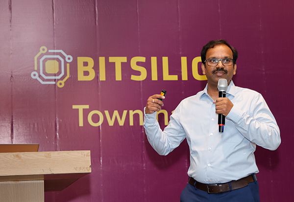
India’s semiconductor ambitions are entering an important new phase.
As artificial intelligence, high-performance computing, automotive electronics, advanced connectivity, and edge computing reshape the global technology landscape, the demand for increasingly sophisticated silicon continues to accelerate. At the same time, India is strengthening its position not only as a source of engineering talent, but as an ecosystem capable of contributing more deeply to semiconductor design, intellectual property, and technology innovation.
Against this backdrop, BITSILICA and its Co-Founder & CEO, Bhaskar Kakani, have recently been featured in two prominent stories — one by IIIT Hyderabad and another by The New Indian Express.
Together, the two features offer complementary perspectives on the journey — from the experiences that shaped an engineer and entrepreneur to the evolution of BITSILICA as a semiconductor engineering organization.
From IIIT Hyderabad to the Semiconductor Industry
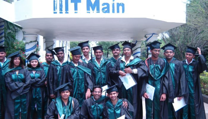 Bhaskar Kakani’s semiconductor journey has strong roots in engineering education.
An alumnus of IIIT Hyderabad’s M.Tech program in VLSI & Embedded Systems, Bhaskar built his foundation in chip design through advanced coursework, research-oriented learning, and exposure to complex engineering challenges.
His professional journey subsequently took him through semiconductor technology roles involving areas such as verification, FPGA platforms, PCIe solutions, and complex SoC development.
But the path was not entirely linear.
At one stage, Bhaskar stepped away from a promising technology career to pursue the Civil Services examination. While that journey did not lead to the outcome originally intended, the experience broadened his perspective beyond technology and eventually became part of the foundation for his entrepreneurial ambitions.
Those experiences — engineering, setbacks, learning, business exposure, and a growing understanding of the semiconductor ecosystem — eventually converged into the journey behind BITSILICA.
Building BITSILICA
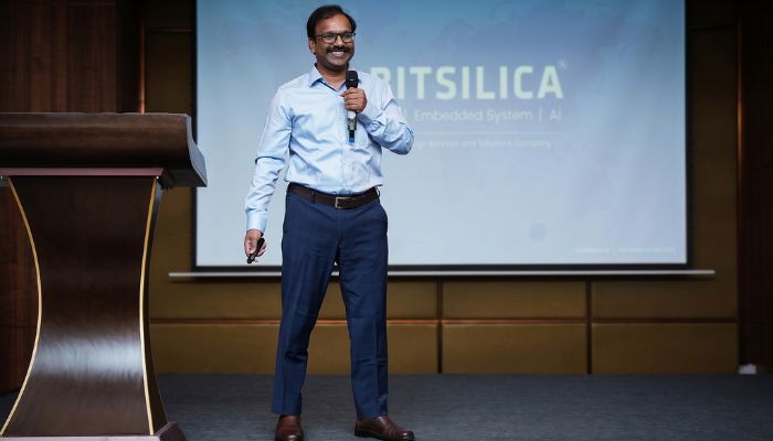 BITSILICA began in 2019–20 with a small engineering team and a clear ambition: to build a world-class semiconductor engineering R&D organization.
The company entered the market at a particularly demanding time, just before the disruption created by the global pandemic.
What followed was a period of capability building and expansion.
From its beginnings with a small team, BITSILICA has grown into a global semiconductor engineering organization with hundreds of engineers working across India and international locations.
Along the way, the organization has expanded its engineering capabilities across multiple areas of the semiconductor development lifecycle, including ASIC Design, Design Verification, Physical Design, Design for Test (DFT), FPGA Design, Embedded Systems & Software, Silicon Validation, and Systems Engineering.
This growth represents more than an increase in scale. It reflects a progression toward taking responsibility for increasingly complex semiconductor engineering programs.
Why Semiconductor Engineering Demands More Than Scale?
Modern chip development leaves very little room for error.
Semiconductor programs involve long development cycles, significant investment, advanced process technologies, and highly specialized engineering teams. A problem discovered after silicon fabrication can have consequences far beyond a conventional software defect.
For semiconductor engineering organizations, success therefore depends not simply on the number of engineers available.
It requires deep domain expertise, specialized engineering capabilities, the ability to scale teams at the right stages of a program, continuous adaptation to evolving technologies, and consistent execution across the silicon development lifecycle.
As semiconductor architectures become more sophisticated, engineering organizations must evolve with them.
AI Is Changing the Silicon Landscape
One of the most significant forces reshaping semiconductor design today is Artificial Intelligence.
The computing industry has moved beyond a world dominated primarily by general-purpose processors. GPUs, AI accelerators, specialized compute architectures, advanced memory technologies, and heterogeneous computing platforms are becoming increasingly important to modern AI workloads.
This shift is also changing what semiconductor companies require from their engineering partners.
Design complexity is increasing. Compute requirements are rising. Memory architectures are evolving. New accelerators and heterogeneous architectures require specialized expertise across multiple stages of silicon development.
For BITSILICA, this evolution closely aligns with its focus on advanced semiconductor engineering and next-generation computing platforms.
From Engineering Execution to Greater Technology Ownership
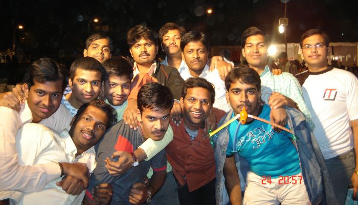 India has long been recognized for its semiconductor engineering talent.
The next opportunity is to translate that engineering strength into greater participation in semiconductor architecture, intellectual property, products, and technology innovation.
That transition is challenging.
Building semiconductor IP and products requires significant capital, experienced architects, long development cycles, access to advanced technologies, and the ability to manage substantial technical and commercial risk.
At the same time, India’s semiconductor ecosystem is evolving.
Growing industry-academia collaboration, semiconductor initiatives, startup activity, and global investment are creating opportunities for the country to participate more deeply across the semiconductor value chain.
BITSILICA’s journey reflects this broader ambition to build deeper engineering capabilities and contribute to increasingly complex semiconductor programs.
Building the Talent Behind the Technology
Semiconductor progress ultimately depends on people.
Advanced tools and process technologies are critical, but designing complex silicon requires engineers with strong fundamentals, specialized domain knowledge, practical experience, and the ability to continuously learn as architectures evolve.
This makes collaboration between industry, academia, research institutions, and the broader semiconductor ecosystem especially important.
Bhaskar Kakani’s own journey — from IIIT Hyderabad to semiconductor engineering, entrepreneurship, and his role today as Co-Founder & CEO of BITSILICA — highlights the importance of combining strong technical foundations with long-term industry experience.
Developing semiconductor talent and creating opportunities for engineers to work on challenging real-world programs remain important parts of building a stronger semiconductor ecosystem.
Entering the Next Chapter
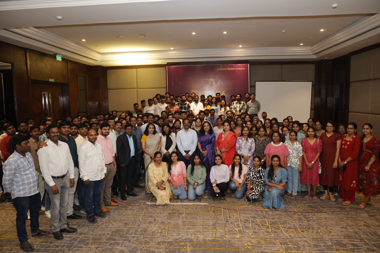 A major milestone in BITSILICA’s journey came with the company becoming part of Quest Global.
The combination opens opportunities to contribute to increasingly complex semiconductor programs and broader engineering solutions while building on BITSILICA’s deep semiconductor expertise.
For BITSILICA, the direction remains centered on the industry that shaped its beginnings: semiconductor design and engineering.
But the scope continues to evolve — from scaling engineering teams to delivering project-based solutions, from execution toward greater ownership, and from a small founding team toward participation in complex global semiconductor programs.
Engineering the Future, One Chip at a Time
Bhaskar Kakani’s journey and BITSILICA’s evolution reflect a broader transformation taking place within India’s semiconductor ecosystem.
It is a story built not around a single breakthrough, but around years of engineering, learning, resilience, team building, and a willingness to take on increasingly difficult technology challenges.
As AI creates new demand for specialized compute and India works toward deeper participation in global semiconductor innovation, the opportunity ahead is significant.
For BITSILICA, the mission continues: build deep engineering capability, nurture semiconductor talent, take ownership of increasingly complex programs, and contribute to the technologies shaping the next generation of computing.
Featured Coverage
IIIT Hyderabad — Bhaskar Kakani’s Journey
Read the full IIIT Hyderabad feature on Bhaskar Kakani
The feature explores Bhaskar Kakani, Co-Founder & CEO of BITSILICA, from his M.Tech journey in VLSI & Embedded Systems at IIIT Hyderabad through his semiconductor career, entrepreneurial journey, the creation of BITSILICA, and his perspective on building semiconductor talent and capabilities in India.
The New Indian Express — “BITSILICA: Chipping into the Future”
Read “BITSILICA: Chipping into the Future” — The New Indian Express
The interview explores BITSILICA’s growth, the complexity of modern semiconductor development, the impact of AI on chip architectures, India’s opportunity to build greater semiconductor technology and IP ownership, and the road ahead for the company.
