

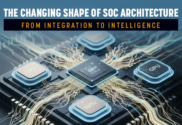
The Changing Shape of SoC Architecture: From Integration to Intelligence
The evolution of the system-on-chip (SoC) has always reflected the evolution of computation itself. From the first single-chip microcontrollers to today’s billion-transistor heterogeneous monsters, SoC design has moved through distinct eras – each driven by a dominant constraint: cost, power, performance, or lately, data movement and intelligence.
For decades, the success of a chip was measured by how much logic you could integrate and how fast it could run. But in the post-Moore world, that yardstick is losing meaning. We’re entering an age where intelligence per watt is replacing transistors per die as the ultimate metric. This shift is not cosmetic – it’s architectural, methodological, and even philosophical.
Let’s explore that arc: from traditional integration, through intent-driven design, to the intelligent SoC that is now beginning to emerge.
1. The Traditional SoC: Integration as an End in Itself
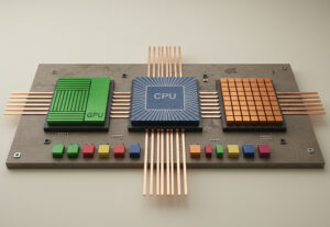
During the 2000s and early 2010s, SoC design was dominated by one objective – integration. The driving question was: How much functionality can we fit onto a single die?
A typical SoC followed a highly modular and hierarchical pattern:
- A general-purpose CPU cluster at the center
- A fixed-function GPU for graphics and compute
- Peripherals (USB, PCIe, UARTs, etc.) stitched through an AXI or AHB bus
- Power and clock controllers around the periphery
- A memory subsystem tuned for bandwidth balancing
Integration meant reducing external components – “one chip does it all.” Verification and design methodologies like UVM were built around this modular structure. Each IP block had clear boundaries, standardized interfaces, and its own verification plan.
This approach made sense in the Moore’s Law era, when scaling down the process node could continuously deliver cost and performance benefits. The design abstraction was IP-centric, and success came from mastering reuse and interface compliance.
However, as SoCs grew past 100+ IPs and multi-billion gate counts, two realities emerged:
- Integration alone didn’t guarantee system performance – data movement became the bottleneck.
- Verification and validation effort grew superlinearly – subsystem-level bugs became dominant.
The SoC had hit a ceiling – not in transistors, but in architectural coherence.
2. The Modern SoC: From Integration to Intent

The inflection point came when workloads began dictating architecture. Mobile AI, edge inference, and cloud-scale training each demanded different compute-to-memory-to-IO ratios. Suddenly, a CPU-GPU pair wasn’t enough.
Today’s SoC design philosophy begins with intent: understanding the end-to-end workload and designing the SoC around dataflow, not around IP reuse.
Instead of integrating more IPs, architects now:
- Partition data across compute clusters (CPU, GPU, NPU) based on latency sensitivity.
- Introduce domain-specific accelerators – NPUs, ISP pipelines, crypto and security islands.
- Reorganize interconnects into coherent fabrics (Arm CMN-700, CHI, AMBA 5).
- Adopt unified memory to reduce data copying and energy waste.
- Treat firmware and runtime software as co-design artifacts, not afterthoughts.
For example, the Apple M-series SoCs, Qualcomm’s Snapdragon X, and NVIDIA’s GH200 all exemplify this intent-driven architecture. Each is tuned for a purpose – whether sustained AI workloads, heterogeneous compute, or memory locality – rather than generic processing.
Power management has also evolved from static to activity-aware, enabling real-time trade-offs between performance and thermal limits based on workload prediction models.
Verification has followed suit. Traditional coverage-driven approaches are giving way to scenario-based verification, where intent models (via Portable Stimulus, PSS 3.0) define how the SoC should behave under realistic system conditions – cache coherency, QoS arbitration, or partial subsystem power collapse.
3. The Intelligent SoC: Architecture That Learns and Adapts

The next frontier is not just about designing for AI – it’s about designing with AI.
Intelligence is entering the SoC at multiple levels:
- Hardware: Embedded NPUs and adaptive compute fabrics that adjust precision, clocking, and routing based on workload type (e.g., Intel’s NPU in Lunar Lake or AMD’s AI Engine in Versal).
- System-level control: Predictive power and thermal management based on real usage telemetry, rather than pre-set tables.
- Verification and design tools: Agentic AI systems (like ChipAgents and Synopsys.ai) that learn failure patterns, optimize regressions, and even generate verification stimuli automatically.
In an intelligent SoC, the architecture itself participates in optimization loops – monitoring behavior, learning from it, and adjusting dynamically.
This requires self-describing hardware – IPs that expose intent metadata, telemetry hooks, and controllable policies. Protocols like CXL, CHI-E, and UCIe 2.0 are evolving in this direction, defining how components communicate their capabilities, not just their interfaces.
The fabric becomes a brainstem, not just a bus. It routes, prioritizes, predicts, and sometimes throttles – autonomously.
Verification, again, must evolve. Instead of static assertions, we now talk about adaptive verification – environments that co-simulate firmware, runtime policies, and AI behavior models. Verification is no longer about “did it do what we coded?” but “does it keep doing what we intended, as it adapts?”
4. Traditional vs. Modern vs. Future SoC – A Comparative Snapshot