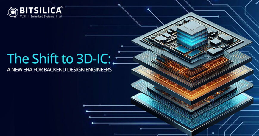
The Shift to 3D-IC: A New Era For Backend Design Engineers
The semiconductor industry’s shift from traditional 2D scaling to three-dimensional integrated circuits (3D-ICs) is transforming chip design. By stacking silicon layers vertically, 3D-ICs deliver significantly higher device density, performance, and energy efficiency—all essential for advancing AI, high-speed computing, and mobile technologies. However, while 3D-ICs offer enormous potential, they introduce fresh challenges for backend design engineers, requiring innovative approaches to manage power, thermal, and signal integrity issues.
How are 3D-IC Different?
In 3D-ICs, dies are either stacked or interconnected using Through-Silicon Vias (TSVs). This enables ultra-compact, high-performance designs by shortening data paths and increasing processing speeds. Yet, building “up” rather than “out” also adds design complexities in backend processes, impacting areas like power distribution, thermal management, and layout optimization.
Core Challenges in 3D-IC Backend Design
1. Through-Silicon Via (TSV) Integration
TSVs serve as the electrical backbone for 3D-IC layers but bring new layout demands:
• Placement and Area: TSVs occupy valuable die area, limiting flexibility in design layouts.
• Thermal Management: The high power density near TSVs can generate hotspots, requiring careful placement.
• Design Constraints: Meeting TSV-specific design rules means additional routing and layout complexities.
2. Thermal Management
Each layer in a 3D-IC adds thermal resistance, creating potential hotspots that can impact reliability. Backend engineers need to explore solutions such as thermal vias, heat spreaders, and thermally efficient materials to enhance heat dissipation across layers.
3. Power Distribution and IR Drop
Stacked layers increase power density, complicating power distribution. Engineers must create robust power networks, strategically positioning TSVs to stabilise power delivery without excessive IR drop, which could jeopardise device reliability.
4. Signal Integrity and Crosstalk
Vertical stacking amplifies the risk of signal integrity issues, like crosstalk and EMI, between closely packed layers. Optimised routing, strategic TSV placements, and shielding techniques are essential to reduce interference and maintain communication reliability across layers.
Tools and Techniques for 3D-IC
To tackle these challenges, backend engineers need to embrace new tools and methodologies:
• Thermal-Aware Placement and Routing: Advanced EDA tools enable engineers to manage heat distribution, guiding component placement across layers to minimise thermal hotspots.
• Power Network Optimization: Power-aware routing tools optimise TSV placement and power delivery, reducing IR drop and supporting stable performance.
• Signal Integrity Analysis: EMI and crosstalk analysis tools assist in identifying interference risks, allowing engineers to refine routing paths and shielding strategies.
Backend Engineers in 3D-IC
Despite its challenges, 3D-IC offers backend engineers new opportunities:
Explore More: The Role of Place and Route in VLSI Physical Design


