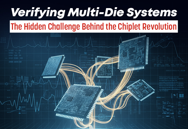
Verifying Multi-Die Systems: The Hidden Challenge Behind the Chiplet Revolution
In recent years, the semiconductor industry has started talking less about single giant chips and more about chiplets. The idea is simple in concept but revolutionary in impact – instead of building one massive die with every function squeezed in, you split the design into multiple smaller dies, each optimized for what it does best, and then connect them together inside the same package.
This new way of thinking has made it possible to go beyond the limits of a single silicon die. Companies like AMD, Intel, and Apple are already doing it at scale. But as the physical design of these multi-die systems matures, a quieter problem has started to dominate conversations inside engineering teams – how do you actually verify that all these dies work correctly together?
When you move from one die to many, verification complexity doesn’t just double – it explodes. And this is where most design teams are realizing that traditional verification flows simply don’t scale anymore.
The Reality Behind Multi-Die Verification
Paul Graykowski from Cadence Design Systems summed it up neatly in his Semiconductor Engineering talk: the industry has spent years refining the physical side of chiplets – packaging, interposers, interconnect standards – but the verification side has not received the same attention.
In theory, each die can be verified on its own. In practice, that’s not enough. A perfectly verified chiplet can still fail when placed next to another die, because the combined system behaves differently. Timing, latency, data ordering, and power behavior across dies create new bugs that single die testing never reveals.
Let’s take a real example. Suppose you have a compute die and a memory die connected through a Universal Chiplet Interconnect Express (UCIe) interface. Both are verified separately – all good. But when integrated, slight timing drift or synchronization lag might cause rare transaction failures under high bandwidth. This sort of bug might appear only after billions of cycles – or worse, only on silicon.
That’s why multi-die verification isn’t just an extension of SoC verification. It’s a new discipline in itself.
Why It’s Harder Than It Sounds?
There are a few reasons why verification becomes harder in chiplet-based systems:

Scalability is the first one. Simulating a single large SoC already stretches compute resources. When you add more dies, simulation size, memory requirements, and runtime all explode. A monolithic testbench that includes everything often cannot even compile, let alone run efficiently.
Cross-vendor integration is another big hurdle. In the chiplet world, not every die comes from the same company. Two vendors might provide verified dies, but their simulation models, testbenches, and verification environments may not align. Connecting them is like trying to plug together two different computer games and expecting them to share the same save file.
Then comes synchronization. Each die might have its own clock domains, resets, and handshake protocols. When they’re simulated together, keeping them in sync without killing performance is extremely hard. If you force too tight synchronization (every clock edge), simulations slow to a crawl. If you go too loose, you lose accuracy. Finding that balance is a constant struggle.
Finally, there’s time pressure. Verification can’t wait for the packaging or interposer design to be finalized. Teams have to test cross-die communication much earlier in the design flow, often when the only things available are virtual models or behavioral abstractions.
This is why the industry talks about “shifting verification left” – starting it earlier, before physical prototypes exist. Doing this well can be the difference between first-silicon success and months of re-spins.
Cadence’s Distributed Verification Method

To handle all this, Cadence has developed what it calls a distributed verification approach. The key idea is to divide and conquer.
Instead of building one huge simulation environment that contains all the dies, each die runs in its own simulation process – on its own core, or even on a separate machine. These simulation instances communicate through what Cadence calls virtual channels.
Think of it like two actors performing in separate studios, connected by a live video feed. They interact in real time, but they don’t need to be in the same room. The system synchronizes only when necessary – for example, when a data transaction crosses from one die to another.
This “transaction-based synchronization” avoids the bottleneck of forcing every clock cycle to line up across dies. It also allows simulation to scale efficiently, distributing workloads across multi-core servers or even cloud machines.
What’s elegant about this approach is that it doesn’t discard existing verification work. The testbenches used for each die can mostly be reused with minimal changes – maybe adjusting memory maps or adding channel definitions. Teams don’t have to rebuild their entire verification environment from scratch.
Cadence’s results show that this distributed setup can achieve up to three times faster performance than traditional monolithic simulations. But more importantly, it lets engineers start system-level verification much earlier, even before interposer and package details are locked down.
What to Verify in a Multi-Die System?

Verifying a multi-die system goes far beyond checking that “the link works.” The real goal is to prove that the system behaves correctly in every realistic scenario, including the rare ones.
For example, you need to ensure that the inter-die link correctly brings itself up, that data integrity is maintained even under retries, that errors are detected and recovered properly, and that cross-die flow control doesn’t cause deadlocks.
If you’re using a standard like UCIe, that means verifying multiple operational modes – raw, streaming, and protocol-based – as well as features like lane repair, CRC replay, and asymmetric link operation.
Power and reset interactions between dies also need careful study. If one die resets while another continues transmitting, the system shouldn’t hang or corrupt data.
Manageability and monitoring are new layers added in UCIe 2.0 and 3.0, allowing firmware-level health reporting, field diagnostics, and even remote firmware updates. These too need verification at the transaction level.
And, of course, there are the physical realities that no digital testbench can ignore – jitter, skew, thermal drift, voltage droop. Cross-die verification has to account for these through co-simulation with thermal, power, and signal-integrity models.
A Practical Verification Flow
In practice, multi-die verification is a multi-phase journey. It often starts with strong die-level verification: each chiplet must be functionally correct and well-constrained for timing and latency. Then, engineers define how dies will communicate – choosing the interface standards (like UCIe or BoW) and specifying data widths, latency targets, and reliability mechanisms.
At this stage, distributed simulation begins. Each die’s verification environment is reused, and virtual channels connect them. Specialized verification IP (VIP) can simulate the UCIe or BoW interface, injecting traffic, monitoring coverage, and flagging protocol violations.
Once functional verification stabilizes, teams move on to multi-physics co-verification. Tools like Cadence Voltus/Celsius or Ansys RedHawk-SC analyze power, IR-drop, electromigration, and thermal coupling across the package. It’s important to verify that no die exceeds thermal limits or suffers IR-drop-induced timing failures when the entire stack operates at full load.
Then comes design-for-test (DFT). Standards such as IEEE 1838 provide a framework to test stacked dies using hierarchical scan paths and flexible test ports. This ensures each die, and the interconnects between them, can be tested before and after stacking.
Finally, verification extends into lifecycle testing – using runtime telemetry, self-test features, and firmware-level health management to monitor chiplets in the field. With UCIe 2.0 and beyond, this kind of manageability is becoming part of the expected design flow.
What the Future Looks Like?

The direction is clear: chiplet-based design is here to stay, and verification methodologies are catching up. The next versions of UCIe, BoW, and IEEE standards are making chiplet systems more interoperable, but also more demanding to verify.
The UCIe 3.0 specification, released in 2025, increases data rates beyond 48 GT/s and adds deeper manageability. It will require even tighter timing models and runtime calibration tests. Meanwhile, new chiplet classes – especially memory and AI accelerators – are introducing heavier bandwidth and power interactions that make cross-die verification more complex than ever.
There’s also a growing focus on system-level telemetry: using field data from deployed systems to refine simulation regressions. This means that in the near future, real-world data will feed back into pre-silicon verification, closing the loop between design and deployment.
The long-term vision is that distributed verification will become standard practice. Teams will routinely run die-level and cross-die simulations in parallel, scaling across local farms or cloud servers, reusing testbenches seamlessly. Verification won’t be a bottleneck – it will be a continuous, integrated process.
Conclusion
Chiplet design is reshaping the semiconductor landscape, but it’s also redefining how we verify complex systems. It’s no longer enough to prove that one die works perfectly – you have to prove that a family of dies behaves like a single, predictable system.
Distributed simulation, early verification, strong DFT infrastructure, and physical co-analysis are now essential ingredients. The goal is simple: catch cross-die problems early, shorten debug cycles, and hit first-silicon success more consistently.
Multi-die verification may still sound niche today, but it’s rapidly becoming the mainstream path for advanced systems. In the coming years, the line between chip and package, between die and system, will keep blurring – and verification will be the glue that holds it all together.

