Chiplet Architectures in AI Accelerators: Breaking the Monolith
Abstract
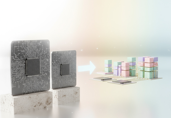
The rise of artificial intelligence has created an insatiable demand for compute, memory, and scale. But the monolithic system-on-chip (SoC) approach that powered decades of semiconductor growth is reaching its physical and economic limits. Reticle boundaries, yield challenges, and thermal constraints make it increasingly impractical to build ever-larger dies. Chiplets — smaller dies integrated into a single package — offer a way forward. They improve yields, lower costs, and enable heterogeneous integration of diverse functions within one package.
This whitepaper explores the history and rationale of chiplets, their use in CPUs and GPUs, their adoption in AI accelerators, and the enabling technologies such as 2.5D interposers, 3D stacking, and UCIe interconnects. It examines how AMD, Intel, Nvidia, and TSMC are pursuing different strategies, and how chiplets could reshape the balance of power in the AI datacenter market. We argue that chiplets represent more than a packaging trend — they are a structural shift that could erode Nvidia’s hardware monopoly and create a more open, multi-vendor future for AI.
1. Background: From Monoliths to Chiplets
The semiconductor industry has long thrived on Moore’s Law, which predicted the doubling of transistors every 18–24 months. Historically, this was achieved by building larger, denser monolithic dies. GPUs epitomized this trend: each new generation delivered bigger chips with more cores, caches, and memory interfaces.
By the mid-2010s, however, cracks began to show. At advanced nodes like 7nm and 5nm, defect densities meant that very large dies suffered poor yields. The reticle limit — the maximum area a photolithography system can expose at once (≈850 mm²) — imposed a hard ceiling. Thermal density also became problematic: one giant die concentrates heat, making cooling harder.
Chiplets arose as a practical solution. By splitting a large design into multiple smaller dies, manufacturers improved yield, allowed process-node optimization, and introduced modularity. This disaggregation has now become central to AI accelerator design, where demands for scale have far outpaced what a single die can deliver.
2. Why Chiplets? Technical and Economic Drivers

2.1 Yield and Cost
The economics of advanced nodes are brutal. A defect on a 600 mm² die destroys the entire chip. On a 100 mm² chiplet, only a fraction of the package is lost. By integrating known-good chiplets, yields improve dramatically.
2.2 Reticle and Power Limits
Photolithography reticle limits prevent building dies larger than ~850 mm². AI workloads demand trillions of transistors, forcing multi-die approaches. Distributing power and thermal load across chiplets also makes cooling more feasible.
2.3 Modularity
Different functions can be fabricated on different nodes. Compute cores on 3nm, I/O dies on 7nm, and analog controllers on 12nm — each optimized for performance and cost.
2.4 Heterogeneous Integration
Chiplets enable hybrid packages: GPUs combined with CPUs, cache, FPGAs, or even domain-specific accelerators. For AI, this means tighter integration of training and inference functions.
3. Use Cases: From CPUs to AI Accelerators

3.1 CPUs Lead the Way
AMD’s Zen 2 CPUs (2019) used multiple compute chiplets linked by Infinity Fabric, with an I/O die handling memory and PCIe. This architecture outperformed Intel’s monolithic CPUs, proving chiplets’ viability.
3.2 GPUs and AI Accelerators
- AMD MI200 (2021): First datacenter GPU with dual-die architecture.
- AMD MI300 (2023): Integrated CPU + GPU + HBM in a 3D-stacked design with >146B transistors.
- Intel Ponte Vecchio (2022): 47 tiles, 5 process nodes, EMIB + Foveros packaging. Complex but pioneering.
- Nvidia Hopper/Blackwell: Remain monolithic, but upcoming Rubin GPUs (2026) expected to adopt chiplets.
3.3 Beyond GPUs
Broadcom and Marvell use chiplets in networking ASICs; Apple uses them in M1 Ultra’s die-to-die interconnect. The model is becoming universal across compute domains.
4. Deep Dive Technologies
4.1 2.5D Interposers
Large silicon interposers host multiple dies side-by-side, connected by high-density wiring. AMD’s MI200 and MI300 use TSMC’s CoWoS interposer technology.
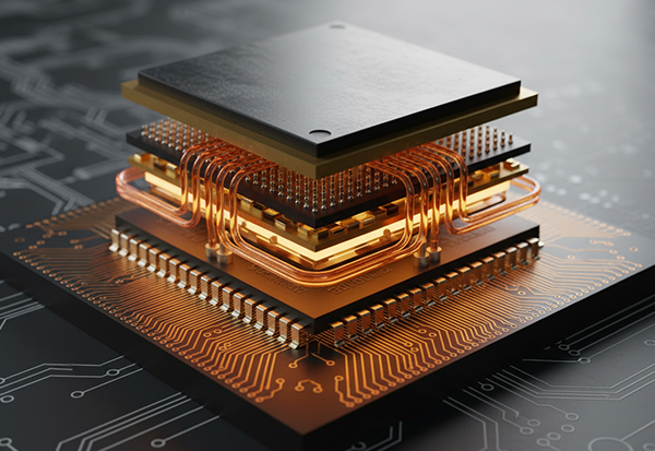
4.2 3D Stacking and Hybrid Bonding
Dies are stacked vertically, with hybrid bonding providing dense interconnects. AMD’s 3D V-Cache (2021) stacked cache directly on CPU cores; MI300 stacked compute with HBM.
4.3 Advanced Packaging Platforms
- AMD Infinity Fabric: Proprietary, scalable.
- Intel EMIB + Foveros: Embedded bridges + die stacking.
- TSMC SoIC: Hybrid bonding for 3D ICs.
- UCIe: Industry standard for cross-vendor chiplet interconnect.
4.4 Thermal and Power Management
Backside power delivery, liquid cooling, and new materials are being explored to address thermal constraints of chiplet packages.
5. Key Players
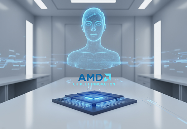
- AMD: Chiplet pioneer. Leads in CPU and GPU chiplets, leveraging TSMC packaging.
- Intel: Innovator in packaging. Ponte Vecchio was ambitious; UCIe leadership gives it influence.
- Nvidia: Reluctant adopter. Monolithic approach still dominant, but future Rubin GPUs will shift.
- TSMC: Critical enabler. Provides CoWoS/SoIC capacity; a bottleneck for the global AI supply chain.
- Samsung / SK Hynix / Micron: Memory vendors integrating HBM into chiplet-based packages.
6. Breaking the Monopoly
Chiplets create opportunities to challenge Nvidia’s dominance:
- Open Standards (UCIe): Could allow GPU dies, accelerator chiplets, and memory dies from different vendors to interoperate.
- Third-Party Innovation: Specialized startups could supply chiplets (e.g., for compression, security, or inference).
- Supply Chain Resilience: Disaggregation allows multi-fab sourcing, reducing dependency on single vendors.
For AMD, chiplets are a strategic weapon to counter Nvidia’s monolithic dominance. For hyperscalers, chiplets promise lower costs and multi-vendor flexibility.
7. Challenges
- Latency: Cross-chiplet communication still slower than on-die.
- Software: CUDA optimized for monolithic GPUs; ROCm must evolve to abstract chiplets effectively.
- Packaging Costs: Interposers and 3D stacks are expensive and thermally challenging.
- Standardization: Nvidia resists UCIe; industry must rally around open standards.
8. Future Directions

Chiplets will reshape AI hardware in three ways:
- Trillion-Transistor Packages: Multi-die systems with CPUs, GPUs, and memory stacked.
- Open Multi-Vendor Packages: UCIe enabling composable packages from different vendors.
- Specialized Acceleration: Domain-specific chiplets (AI inference, cryptography) added into packages.
By 2030, packages with 1 trillion transistors, 2–3 TB/s bandwidth, and 10+ HBM stacks could be mainstream, all enabled by chiplet technology.
Conclusion
Chiplets are not just an economic fix; they are a paradigm shift. They make possible what monolithic dies cannot: scaling beyond reticle limits, integrating heterogeneous compute, and opening the door to multi-vendor collaboration. AMD has proven their value, Intel is pushing packaging innovation, TSMC is the indispensable enabler, and Nvidia is being forced to adapt.
If the industry embraces open standards like UCIe, chiplets could break Nvidia’s monopoly in the same way Ethernet is challenging InfiniBand and UALink challenges NVSwitch. The future of AI will not be determined by the fastest GPU alone, but by how chiplets redefine the package as the true unit of innovation.

